- 您现在的位置:买卖IC网 > Sheet目录337 > LT3492IFE#TRPBF (Linear Technology)IC LED DVR HP CONST CURR 28TSSOP
�� �
�
�LT3492�
�APPLICATIONS� INFORMATION�
�this� capability.� Some� margin� to� data� sheet� limits� is� included,�
�along� with� provision� for� 200mA� inductor� ripple� current.�
�For� boost� mode� converters:�
�Thermal� Considerations�
�The� LT3492� is� rated� to� a� maximum� input� voltage� of� 30V�
�for� continuous� operation,� and� 40V� for� nonrepetitive� one�
�I� OUT(MAX)� ?� 0.4A�
�V� IN(MIN)�
�V� OUT(MAX)�
�second� transients.� Careful� attention� must� be� paid� to� the�
�internal� power� dissipation� of� the� LT3492� at� higher� input�
�voltages� and� higher� switching� frequencies/output� voltage�
�I� OUT(MAX)� ?� 0.4A�
�For buck mode converters:�
�I� LED(MAX)� ?� 0.4A�
�For� SEPIC� and� buck-boost� mode� converters:�
�V� IN(MIN)�
�(V� OUT(MAX)� +� V� IN(MIN)� )�
�If� some� level� of� analog� dimming� is� acceptable� at� minimum�
�supply� levels,� then� the� CTRL� pin� can� be� used� with� a� resistor�
�divider� to� V� IN� (as� shown� in� the� Block� Diagram)� to� provide�
�a� higher� output� current� at� nominal� V� IN� levels.�
�The� LED� current� of� each� channel� is� programmed� by� con-�
�necting� an� external� sense� resistor� R� SENSE� in� series� with�
�the� LED� load,� and� setting� the� voltage� regulation� threshold�
�across� that� sense� resistor� using� CTRL� input.� If� the� CTRL�
�voltage,� V� CTRL� ,� is� less� than� 1V,� the� LED� current� is:�
�to� ensure� that� a� junction� temperature� of� 125°C� is� not�
�exceeded.� This� is� especially� important� when� operating�
�at� high� ambient� temperatures.� Consider� driving� V� IN� from�
�5V� or� higher� to� ensure� the� fastest� switching� edges,� and�
�minimize� one� source� of� switching� loss.� The� exposed�
�pad� on� the� bottom� of� the� package� must� be� soldered� to�
�a� ground� plane.� This� ground� should� then� be� connected�
�to� an� internal� copper� ground� plane� with� thermal� vias�
�placed� directly� under� the� package� to� spread� out� the� heat�
�dissipated� by� the� LT3492.�
�Board� Layout�
�The� high� speed� operation� of� the� LT3492� demands� careful�
�attention� to� board� layout� and� component� placement.� The�
�exposed� pad� of� the� package� is� the� only� GND� terminal� of�
�the� IC� and� is� important� for� thermal� management� of� the�
�IC.� Therefore,� it� is� crucial� to� achieve� a� good� electrical� and�
�I� LED� =�
�V� CTRL�
�10� ?� R� SENSE�
�thermal� contact� between� the� exposed� pad� and� the� ground�
�plane� of� the� board.� Also,� in� boost� con?guration,� the�
�Schottky� recti?er� and� the� capacitor� between� GND� and� the�
�I� LED� =�
�If V� CTRL� is higher than 1V, the LED current is:�
�100mV�
�R� SENSE�
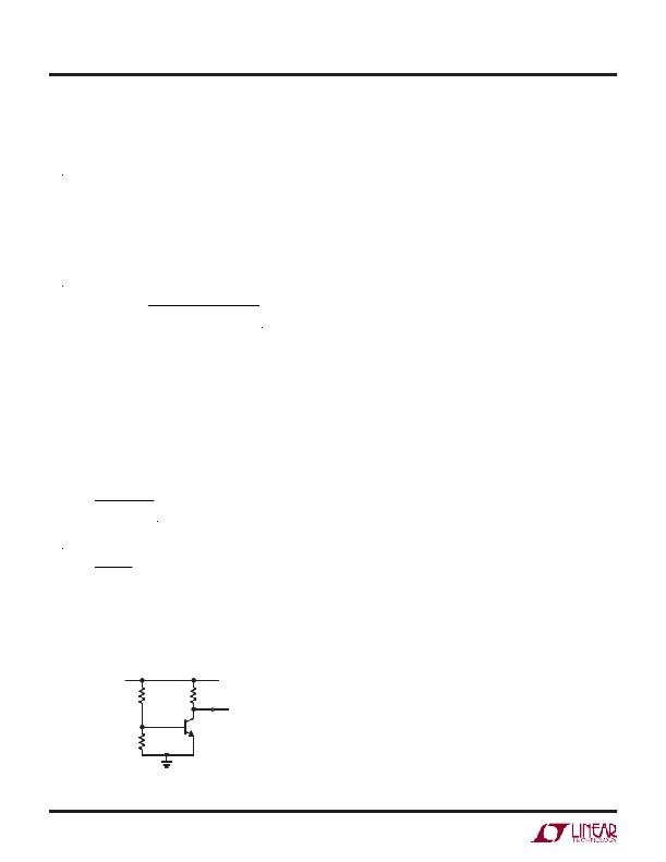
�The� CTRL� pins� should� not� be� left� open.� The� CTRL� pin�
�can� also� be� used� in� conjunction� with� a� PTC� thermistor� to�
�provide� overtemperature� protection� for� the� LED� load� as�
�shown� in� Figure� 2.�
�cathode� of� the� Schottky� are� in� the� high� frequency� switching�
�path� where� current� ?ow� is� discontinuous.� These� elements�
�should� be� placed� so� as� to� minimize� the� path� between� SW�
�and� the� GND� of� the� IC.� To� reduce� electromagnetic� interfer-�
�ence� (EMI),� it� is� important� to� minimize� the� area� of� the� SW�
�node.� Use� the� GND� plane� under� SW� to� minimize� interplane�
�coupling� to� sensitive� signals.� To� obtain� good� current�
�regulation� accuracy� and� eliminate� sources� of� channel� to�
�channel� coupling,� the� ISP� and� ISN� inputs� of� each� channel�
�V� REF�
�45k�
�2V�
�50k�
�of� the� LT3492� should� be� run� as� separate� lines� back� to� the�
�terminals� of� the� sense� resistor.� Any� resistance� in� series�
�with� ISP� and� ISN� inputs� should� be� minimized.� Avoid� ex-�
�470Ω�
�PTC�
�3492� F02�
�Figure� 2�
�CTRL1-3�
�tensive� routing� of� high� impedance� traces� such� as� OVP� and�
�V� C� .� Make� sure� these� sensitive� signals� are� star� coupled� to�
�the� GND� under� the� IC� rather� than� a� GND� where� switching�
�currents� are� ?owing.� Finally,� the� bypass� capacitor� on� the�
�V� IN� supply� to� the� LT3492� should� be� placed� as� close� as�
�possible� to� the� V� IN� terminal� of� the� device.�
�3492fa�
�12�
�发布紧急采购,3分钟左右您将得到回复。
相关PDF资料
LT3496IUFD#PBF
IC LED DRVR WHT/RGB BCKLT 28-QFN
LT3497EDDB#TRMPBF
IC LED DRIVR WHITE BCKLGT 10-DFN
LT3498EDDB#TRPBF
IC LED DRVR WT/OLED BCKLGT 12DFN
LT3517HUF#PBF
IC LED DRIVER AUTOMOTIVE 16-QFN
LT3519EMS-2#PBF
IC LED DRVR HP CONST CURR 16MSOP
LT3590ESC8#TRMPBF
IC LED DRVR WHITE BCKLGT SC-70-8
LT3591EDDB#TRMPBF
IC LED DRIVER WHITE BCKLGT 8-DFN
LT3593ES6#TRMPBF
IC LED DRIVR WHITE BCKLGT TSOT-6
相关代理商/技术参数
LT3492IFEPBF
制造商:LINER 制造商全称:Linear Technology 功能描述:Triple Output LED Driver with 3000:1 PWM Dimming
LT3492IFETRPBF
制造商:LINER 制造商全称:Linear Technology 功能描述:Triple Output LED Driver with 3000:1 PWM Dimming
LT3492IUFD
制造商:LINER 制造商全称:Linear Technology 功能描述:Triple Output LED Driver with 3000:1 PWM Dimming
LT3492IUFD#PBF
功能描述:IC LED DRIVER TRIPLE 28QFN RoHS:是 类别:集成电路 (IC) >> PMIC - LED 驱动器 系列:- 标准包装:6,000 系列:- 恒定电流:- 恒定电压:- 拓扑:开路漏极,PWM 输出数:4 内部驱动器:是 类型 - 主要:LED 闪烁器 类型 - 次要:- 频率:400kHz 电源电压:2.3 V ~ 5.5 V 输出电压:- 安装类型:表面贴装 封装/外壳:8-VFDFN 裸露焊盘 供应商设备封装:8-HVSON 包装:带卷 (TR) 工作温度:-40°C ~ 85°C 其它名称:935286881118PCA9553TK/02-TPCA9553TK/02-T-ND
LT3492IUFD#TRPBF
功能描述:IC LED DVR TRPL PWM DIM 28TSSOP RoHS:是 类别:集成电路 (IC) >> PMIC - LED 驱动器 系列:- 标准包装:6,000 系列:- 恒定电流:- 恒定电压:- 拓扑:开路漏极,PWM 输出数:4 内部驱动器:是 类型 - 主要:LED 闪烁器 类型 - 次要:- 频率:400kHz 电源电压:2.3 V ~ 5.5 V 输出电压:- 安装类型:表面贴装 封装/外壳:8-VFDFN 裸露焊盘 供应商设备封装:8-HVSON 包装:带卷 (TR) 工作温度:-40°C ~ 85°C 其它名称:935286881118PCA9553TK/02-TPCA9553TK/02-T-ND
LT3492IUFDPBF
制造商:LINER 制造商全称:Linear Technology 功能描述:Triple Output LED Driver with 3000:1 PWM Dimming
LT3492IUFDTRPBF
制造商:LINER 制造商全称:Linear Technology 功能描述:Triple Output LED Driver with 3000:1 PWM Dimming
LT3493
制造商:LINER 制造商全称:Linear Technology 功能描述:1.2A, 750kHz Step-Down Switching Regulator in 2mm × 3mm DFN